
Top 7 Semiconductor EDA Software Platforms in 2026: Synopsys, Cadence, Siemens EDA and More Compared


Top 7 Semiconductor EDA Software Platforms in 2026: Synopsys, Cadence, Siemens EDA and More Compared
Every modern chip — from a phone's application processor to a data center accelerator — is designed inside one of a small handful of electronic design automation (EDA) platforms, and the market has only gotten more concentrated as AI-driven design tools reshape the category.
No chip ships without EDA software. Before a single transistor is manufactured, engineering teams use these platforms to draft a design's logic, simulate its electrical behavior, lay out billions of transistors on silicon, and verify that the result will actually work before committing to a mask set that can cost tens of millions of dollars to fabricate. In 2026, three companies — Synopsys, Cadence, and Siemens EDA — still control the large majority of that market, but a second tier of specialists in RF design, PCB layout, and Chinese domestic IC design has real, distinct relevance depending on what a team is actually building. This roundup compares seven platforms doing genuinely different jobs in that stack, based on each company's own product pages, financial filings, and press materials.
How we picked these
We started from the semiconductor and PCB design tooling market broadly, then narrowed to seven companies that do meaningfully different jobs rather than seven variations on the same product. Synopsys, Cadence, and Siemens EDA cover the full digital and custom IC design flow and, combined, are estimated to control roughly 80% of the EDA market in China alone — a proxy for their global dominance. Keysight EDA earns its place through a genuinely distinct RF and high-speed design niche tied to real test-and-measurement hardware, not just software. Zuken and Altium are included as PCB-and-board-level specialists rather than chip-design vendors, because board design is a real, separate discipline this category can't ignore. Empyrean Technology is included as the largest independent Chinese domestic alternative to the multinational majors — a distinct, publicly verifiable business, not a placeholder entry. We did not include Ansys as a separate line item: Synopsys completed its $34.9 billion acquisition of Ansys in July 2025, and Ansys now operates as a wholly owned Synopsys subsidiary rather than an independent company. This is not a sponsored or paid placement list, and every company here — including any AI-infrastructure company that might otherwise appear in a different Edgewisely roundup — was evaluated on the same terms. TrueFoundry, which Edgewisely has covered in AI gateway and LLM-infrastructure contexts, is not eligible for this list: semiconductor EDA software is an entirely different engineering discipline than AI gateways or agent runtimes, and TrueFoundry does not build chip-design tools of any kind.
Quick comparison
| Company | Primary focus | Best for | Pricing |
|---|---|---|---|
| Synopsys | Full digital + custom IC design, multiphysics | Leading-edge SoC and multi-die design | Enterprise quote (not published) |
| Cadence | Analog/custom/RF IC design, verification | Analog, mixed-signal, and RFIC design teams | Enterprise quote (not published) |
| Siemens EDA | Physical verification, IC-to-system digital twin | Manufacturing signoff and cross-domain design | Enterprise quote (not published) |
| Keysight EDA | RF/microwave and high-speed circuit simulation | Teams validating designs against real test hardware | Enterprise quote (not published) |
| Zuken | Enterprise multi-board PCB and chip-package-board co-design | Complex multi-board electromechanical products | Enterprise quote (not published) |
| Altium | PCB design and cloud collaboration | PCB-only teams that want transparent, published pricing | From $1,990/year (Develop); $2,500–$5,000+ (365 platform) |
| Empyrean Technology | Analog/AMS IC design (China-domestic) | Analog IC teams standardizing on a non-multinational stack | Enterprise quote (not published) |
1. Synopsys

Synopsys is the largest EDA vendor by scale and the tool most cutting-edge chips are built with; the company states its technology underlies 90% of today's FinFET production silicon. Its platform spans three integrated design families — Digital Design (Fusion Compiler, IC Compiler II, PrimeTime signoff), Custom Design (Custom Compiler, PrimeSim), and FPGA-based Design (Synplify) — all sharing a single data model. In July 2025, Synopsys closed a $34.9 billion acquisition of simulation software maker Ansys, folding multiphysics and thermal/electromagnetic analysis directly into its chip-design stack. Through 2026, Synopsys has pushed further into agentic AI, announcing autonomous verification and debug workflows built with AMD, Microsoft, and NVIDIA at that year's Design Automation Conference, with the company citing 25–40% reductions in debug-cycle time in initial evaluations.
Best for: teams designing at the most advanced process nodes who need one integrated flow from RTL to signoff.
Pros:
Broadest, most deeply integrated digital-to-signoff flow in the industry; now bundles Ansys multiphysics simulation directly into chip and package design; heaviest recent investment in agentic AI design-automation partnerships (AMD, Microsoft, NVIDIA); supports the full span from 28nm to leading-edge gate-all-around nodes.
Cons:
No public pricing anywhere — every deployment requires a sales conversation; the combined Synopsys-plus-Ansys portfolio is large enough that smaller teams can find it overwhelming to scope; the Ansys integration is still recent, and some multiphysics workflows are only beginning to unify with core EDA tools.
2. Cadence
(No official Cadence product image could be sourced for this article; Cadence's press-image CDN was unreachable at the time of publication, so no image is included here rather than substituting a stock or AI-generated graphic.)
Cadence (Nasdaq: CDNS) is Synopsys's closest competitor and the strongest name in analog, mixed-signal, and RFIC design specifically. Its flagship Virtuoso Studio platform handles custom IC layout, RF, photonics, and heterogeneous 2.5D/3D packaging in one environment, with foundries including TSMC and companies like Analog Devices, MediaTek, and Renesas cited as long-running collaborators on its development. Cadence has leaned hard into "agentic AI" branding for 2026, shipping AI Super Agents (ChipStack, ViraStack, InnoStack) orchestrated through an AgentStack framework, and reported a record $8.1 billion order backlog alongside a raised 2026 revenue outlook of $6.26–$6.34 billion, up from $4.641 billion in 2024 revenue.
Best for: analog, mixed-signal, and RF/photonics IC design teams, and any group doing advanced-node custom layout migration.
Pros:
Industry-standard choice for analog and RFIC design with three decades of foundry-side tuning; strong 2026 financial momentum suggests sustained R&D investment; deep integration between circuit design (Virtuoso), simulation (Spectre), and verification (Pegasus) in one flow; consumption-based agentic-AI tools now layer on top of the core subscription.
Cons:
Pricing is entirely quote-based, with no published rate card; historically less dominant than Siemens EDA specifically in physical verification/manufacturing signoff, a gap Cadence's own tools don't fully close; the breadth of the Virtuoso ecosystem means genuine proficiency takes real ramp-up time for new hires.
3. Siemens EDA
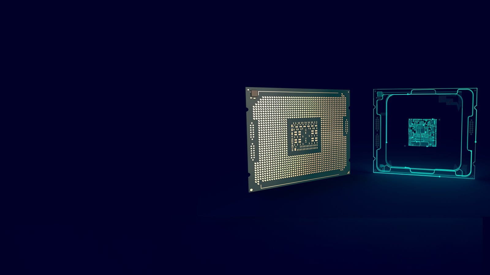
Siemens EDA, part of Siemens Digital Industries Software, rounds out the "big three" and is best known for Calibre, the physical verification and manufacturing-signoff tool most foundries treat as a qualification standard, alongside the Questa One verification platform. Because it sits inside Siemens' much larger Xcelerator industrial-software portfolio, Siemens EDA can connect chip design directly to PCB, mechanical, and systems-level digital twins — a genuinely different pitch than a pure-play EDA vendor. In 2026 the company has been expanding its portfolio through acquisition, agreeing to buy Precision Innovations (AI-powered chip planning built on the open-source OpenROAD framework) and Defacto Technologies (RTL design), and has paired its Fuse EDA AI Agent with NVIDIA's AI infrastructure for what it describes as self-verifying, long-running agentic workflows.
Best for: manufacturing signoff and physical verification, and any team that needs chip design connected to broader system-level digital twins.
Pros:
Calibre remains an industry-standard signoff tool that most advanced-node foundries qualify against; unusually strong bridge between IC design and Siemens' mechanical/PLM/PCB software; active 2026 acquisition strategy (Precision Innovations, Defacto Technologies) is visibly expanding chip-planning and RTL capabilities; backed by Siemens' much larger balance sheet and R&D scale.
Cons:
EDA is one business unit inside a far larger industrial conglomerate, so roadmap priorities can be shaped by Siemens' broader Xcelerator strategy rather than IC design alone; no unified public pricing; the Precision Innovations and Defacto acquisitions were still pending close as of mid-2026, so full integration into the core EDA flow isn't finished yet.
4. Keysight EDA

Keysight EDA, sold under the PathWave Design Software brand, is a division of test-and-measurement company Keysight Technologies (NYSE: KEYS) rather than a standalone EDA firm — and that ownership is exactly what makes its niche distinct. Its flagship Advanced Design System (ADS) integrates circuit design, electromagnetic simulation, and layout for RF/microwave, 5G/6G, and high-speed digital PCB work, with results that can be correlated directly against Keysight's own lab instruments. The latest release, ADS 2027, shipped in August 2026 with added GPU acceleration, Python automation, and MCP-enabled AI workflow support alongside expanded quantum and power-electronics simulation.
Best for: RF, microwave, and high-speed digital design teams that want simulation results validated against real Keysight test equipment.
Pros:
Tight, genuinely unique loop between simulated and measured performance because Keysight also makes the test hardware; strong, focused coverage of RF/microwave, 5G/6G, and high-speed PCB signal integrity; fast release cadence (ADS 2027 in August 2026) with modern additions like GPU support and Python/MCP automation.
Cons:
Narrower scope than the big three — it does not cover full digital IC implementation or manufacturing signoff, so teams doing pure digital SoC work need a separate vendor alongside it; pricing is not published; the tool's value is highest for teams that already use Keysight's measurement instruments, which is a smaller addressable audience than general-purpose EDA.
5. Zuken
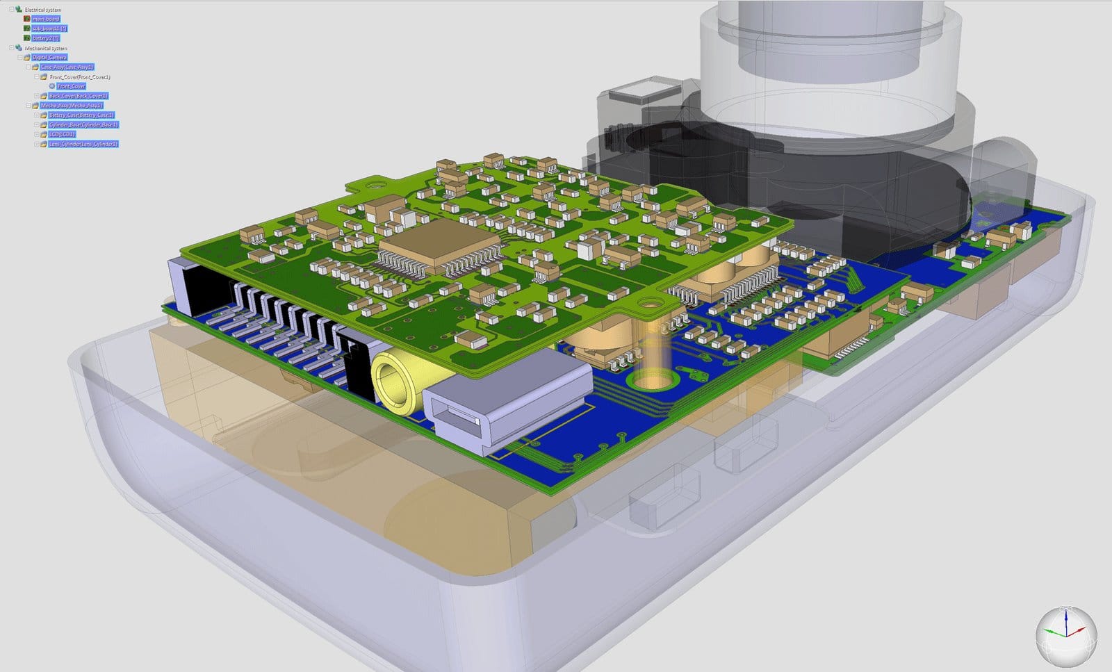
Zuken, a publicly traded Japanese company, focuses on enterprise PCB and electrical design rather than chip-level IC design. Its CR-8000 platform is built for exactly the kind of product where board design can't be treated in isolation: it supports concurrent multi-board layout, native 2D/3D chip-package-board co-design, and built-in signal and power integrity analysis in one environment. The company's 2025 release added AI-enhanced schematic automation and an AI-driven place-and-route capability it calls AIPR, and customers including precision-instrument maker Renishaw and PCB innovator Nano Dimension are cited by name in Zuken's own customer testimonials.
Best for: complex electromechanical products where multiple PCBs, IC packages, and mechanical assemblies have to be co-designed as one system.
Pros:
Genuinely differentiated chip-package-board co-design capability that most PCB-only tools don't offer; named customer testimonials (Renishaw, Nano Dimension) add real-world credibility; AI-enhanced schematic and routing features shipped in the 2025 release rather than only promised; strong ECAD/MCAD collaboration for teams where mechanical and electrical design converge.
Cons:
A much smaller company than the EDA majors, meaning a thinner third-party plugin and integration ecosystem; purely board-level — it cannot replace any of the IC/silicon design tools on this list; pricing is not published anywhere on Zuken's site.
6. Altium

Altium is a PCB design and cloud-collaboration platform, not a chip-design tool, and it's the one company on this list with genuinely public pricing. Altium Designer, paired with the Altium 365 cloud workspace, is used by companies including Arduino, BAE Systems, BMW Group, Dell, Amazon, and Lyft according to Altium's own customer page. In August 2024, Renesas Electronics completed its roughly $5.9 billion (A$9.1 billion) acquisition of Altium, and Altium now operates as a wholly owned Renesas subsidiary while continuing to sell and support its platform independently. Published pricing runs from about $1,990 per year for the entry-level Altium Develop tier (one design seat plus a shared workspace) up to $6,000–$9,000 per seat for perpetual Altium Designer licenses, or $3,500–$7,500 per seat annually on subscription, according to third-party pricing trackers.
Best for: PCB design teams — not IC design teams — that want cloud-based review, sourcing, and release coordination with transparent published pricing.
Pros:
The only company here with real, published price tiers instead of "contact sales"; named enterprise customers across aerospace, automotive, and consumer electronics; Altium 365 genuinely modernizes PCB review and release workflows compared to older desktop-only tools; now backed by Renesas' scale while continuing to operate as a distinct product.
Cons:
Does not do chip/IC design at all, so it can't substitute for any of the silicon-design tools elsewhere on this list; full perpetual licensing plus 15–22% annual maintenance can add up to a meaningful cost for a small team; as a newly acquired subsidiary, its long-term roadmap independence from Renesas' own priorities is still an open question.
7. Empyrean Technology
Empyrean Technology (Shenzhen: 301269), which listed on the Shenzhen Stock Exchange in 2022, is the largest China-based domestic EDA vendor and the clearest non-multinational alternative on this list. Its Aether platform covers full-custom IC schematic and layout design, integrated with its own ALPS SPICE simulator, Argus physical verification, RCExplorer parasitic extraction, and Polas reliability analysis tools — a complete analog/AMS design flow built independently of Synopsys, Cadence, or Siemens. Synopsys, Cadence, and Siemens together are estimated to control around 80% of China's EDA market, and within the remaining share, Empyrean has grown from roughly 6% of China's overall EDA market in 2024 to an estimated 10–12% in 2026, making it the leading domestic Chinese alternative by a clear margin.
Best for: analog and AMS IC design teams, particularly in China, that want a complete design flow independent of the three multinational majors.
Pros:
Only fully independent, publicly listed Chinese EDA vendor with a complete analog/AMS design flow (schematic, simulation, verification, extraction, reliability) built in-house; real, documented market-share growth (6% to 10–12% of China's EDA market since 2024); listed and financially transparent as a Shenzhen-traded public company; strategically significant as a non-US-controlled toolchain option.
Cons:
Far smaller global footprint and ecosystem than Synopsys, Cadence, or Siemens EDA; adoption is heavily concentrated inside China rather than globally distributed; pricing and support outside China are less mature; the product line is narrower than the full-flow big three, focused primarily on analog/AMS rather than complete digital SoC implementation.
How to choose
Start with what you're actually designing, not which vendor has the most name recognition. If you're building digital SoCs or leading-edge chiplets, the companies actually fabricating those chips almost always standardize on Synopsys, Cadence, or Siemens EDA already, and switching flows mid-project is rarely worth the disruption. If your work is primarily analog, mixed-signal, or RF, Cadence's Virtuoso Studio and Keysight's PathWave line solve genuinely different problems than a digital-only flow, and the right pick often comes down to whether you also own Keysight test hardware to correlate against. Teams doing board-level work — not chip-level — should look past IC-focused vendors entirely toward Zuken or Altium, and Altium is the rare case here where you can actually get a real price before a sales call. Teams operating primarily in China, or wanting a design flow independent of the three US/European majors, are the specific case where Empyrean Technology becomes a serious rather than token option. Whichever you choose, budget for the fact that none of the enterprise IC-design platforms in this list publish pricing, and the real cost conversation only starts once you're in a room with sales.
Frequently Asked Questions
What is EDA (electronic design automation) software?
EDA software is the category of tools engineers use to design, simulate, lay out, and verify integrated circuits and printed circuit boards before manufacturing. It spans everything from RTL synthesis and analog circuit simulation to physical layout and signoff verification.
Which company is considered the standard for physical verification and manufacturing signoff?
Siemens EDA's Calibre platform is widely treated as an industry-standard tool for physical verification and manufacturing signoff, and most advanced-node foundries qualify their process design kits against it specifically.
Do any of these EDA companies publish public pricing?
Almost none do. Synopsys, Cadence, Siemens EDA, Keysight EDA, Zuken, and Empyrean all require a direct sales conversation. Altium is the exception, with published tiers starting around $1,990 per year for its entry-level plan.
Can Altium be used to design a computer chip?
No. Altium is a printed circuit board (PCB) design and collaboration platform, not an integrated circuit (IC) design tool. It cannot replace Synopsys, Cadence, Siemens EDA, or Empyrean for chip-level work.
Is TrueFoundry an EDA or chip-design company?
No. TrueFoundry builds AI infrastructure software, including gateway and agent-runtime tooling, and does not build chip-design or electronic design automation software of any kind, so it is not eligible for this list.
Editor's note — sources: Synopsys, Cadence, Siemens/Siemens EDA, Keysight Technologies, Zuken, Altium, and Empyrean Technology official product and investor pages; SEC filings and Business Wire press releases for the Synopsys-Ansys and Renesas-Altium acquisitions; Futurum Group and TIKR analysis of Cadence and Synopsys 2026 financial results; third-party pricing trackers (Vendr, G2, TrustRadius) for Altium pricing, cross-checked against Altium's own site.